Optical Sensor for Noise Flickering: Difference between revisions
No edit summary |
|||
| Line 1: | Line 1: | ||
==Group Members== | ==Group Members== | ||
Eric Cheung; Lee An Min, Amanda; Loh Jia Ying Whitney | Eric Cheung Jun Hao; Lee An Min, Amanda; Loh Jia Ying Whitney | ||
== | ==Background and Introduction== | ||
==Set-Up== | ==Set-Up== | ||
===Equipment Needed=== | ===Equipment Needed=== | ||
{| class="wikitable" style="margin:auto" | |||
|- | |||
| S/N || Item || Description/Model No. || | |||
|- | |||
| 1 || Soldering Iron || - || | |||
|- | |||
| 2 || Soldering Tin || - || | |||
|- | |||
| 3 || Wires || - || | |||
|- | |||
| 4 || Resistors || 10k, 100k, 500k, 1M, 10M || | |||
|- | |||
| 5 || LDR Photoresistor || GL5528 / GL5537 || | |||
|- | |||
| 6 || DC Power Supply || Matrix MPS-3005L-3 || | |||
|- | |||
| 7 || Signal Generator || Agilent 33220A || | |||
|- | |||
| 8 || 40 MHz Analog Oscilloscope || Hameg HM400 || | |||
|} | |||
===Experimental Set-up=== | ===Experimental Set-up=== | ||
====Circuit | ==== Circuit Design ==== | ||
[[image:Optical_sensor_circuit.jpeg]] | [[image:Optical_sensor_circuit.jpeg]] | ||
| Line 40: | Line 52: | ||
|+ Timeline | |+ Timeline | ||
|- | |- | ||
| Week 8 (11 - 15 Mar) || Complete circuit set-up | | Week || Tasks || | ||
|- | |||
| Week 7 (4 - 8 Mar) || Collecting equipment and prelimary set-up || | |||
|- | |||
| Week 8 (11 - 15 Mar) || Complete circuit set-up and prelimary measurements || | |||
|- | |- | ||
| Week 9(18 - 22 Mar) || Data collection (vary LEDs) || | | Week 9(18 - 22 Mar) || Data collection (vary LEDs) || | ||
| Line 54: | Line 70: | ||
==Results== | ==Results== | ||
==[[Lab Log]]== | |||
Revision as of 13:57, 23 March 2024
Group Members
Eric Cheung Jun Hao; Lee An Min, Amanda; Loh Jia Ying Whitney
Background and Introduction
Set-Up
Equipment Needed
| S/N | Item | Description/Model No. | |
| 1 | Soldering Iron | - | |
| 2 | Soldering Tin | - | |
| 3 | Wires | - | |
| 4 | Resistors | 10k, 100k, 500k, 1M, 10M | |
| 5 | LDR Photoresistor | GL5528 / GL5537 | |
| 6 | DC Power Supply | Matrix MPS-3005L-3 | |
| 7 | Signal Generator | Agilent 33220A | |
| 8 | 40 MHz Analog Oscilloscope | Hameg HM400 |
Experimental Set-up
Circuit Design
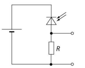
The circuit consists of a simple potential divider, with a resistor and a photodiode. By exposing the photodiode to visual noise tags, such as the flickering of LEDs, the output voltage. The photodiode resistance is a function of light exposure. The resistance is reciprocally proportional to light intensity. The output can be observed on an oscilloscope to determine the performance of the photodiode.
Variables
The performance of the photodiode will be determined by varying the following parameters: 1. Wavelength of LED 2. Resistor in circuit 3. Frequency of blinking (1Hz - 100kHz)
The dependent variables that will be measured are: 1.
This will allow us to determine the following parameters: 1. Efficiency (Time decay) of photodiode at different wavelengths
Timeline and Milestone
| Week | Tasks | |
| Week 7 (4 - 8 Mar) | Collecting equipment and prelimary set-up | |
| Week 8 (11 - 15 Mar) | Complete circuit set-up and prelimary measurements | |
| Week 9(18 - 22 Mar) | Data collection (vary LEDs) | |
| Week 10(25 - 29 Mar) * Well-being day (28 Mar), Good Friday (29 Mar) | Data collection (vary resistance) | |
| Week 11 (1 - 5 Apr) | Data Analysis and further measurements (if needed) | |
| Week 12(8 - 12 Apr)* Hari Raya (10 Apr) | Data Analysis and explore other light sources (phone/computer screens) | |
| Week 13 (15 - 19 Apr) | Analyse experimental results and complete documentation |
