EA Spectroscopy as a series of sensors: Investigating the Impact of Solvent Type on Mobility in Organic Diodes: Difference between revisions
| Line 8: | Line 8: | ||
==Introduction== | ==Introduction== | ||
1 Fundamentals of polymer organic semiconductors | |||
Organic semiconductors are a class of materials composed of organic molecules or polymers that possess semiconductor-like energy levels and are capable of transporting electrical charges. Compared with inorganic semiconductors, organic semiconductors offer advantages such as structural tunability, solution processability, and compatibility with flexible electronic devices[8]. Among them, polymer are particularly important because their long-chain molecular structures enable good film-forming ability and make them highly suitable for large-area solution processing. | |||
PBDB-T is a representative polymer that has attracted significant attention due to its excellent optoelectronic properties and widespread use in organic electronic devices, especially organic solar cells. Structurally, PBDB-T consists of repeating molecular units that form a conjugated polymer backbone. The conjugated backbone plays a central role in determining the semiconducting behavior of the material, as it governs the energy levels and facilitates charge transport along the polymer chain. In addition, PBDB-T contains alkyl side chains attached to the backbone. These side chains mainly improve the solubility and processability of the polymer, which are essential for solution-based fabrication methods. Therefore, the molecular structure of PBDB-T, including its repeating units, conjugated backbone, and side chains, provides the basis for understanding its aggregation behavior, film formation, and charge-transport properties. | |||
2 Basic device for organic semiconductor research | |||
In studies of organic semiconductors, organic diodes are fundamental devices for investigating charge-transport behavior. Typically, an organic diode consists of an ITO anode, a metal cathode, and an organic semiconductor thin film sandwiched between the two electrodes. | |||
To achieve the highest efficiency, we usually utilize hole injection layer and electron injection layer to make sure of the efficient charge injection at both hole and electron contacts, which is guaranteed by the match of the energy levels of these various layers. | |||
The work function is the minimum energy required to move an electron from the Fermi level to the vacuum level. The injection barrier is the energy difference that carriers must overcome in order to be injected from an electrode into the organic semiconductor. Meanwhile, in organic semiconductor diodes, an Ohmic contact refers to a contact at which the carrier injection and collection resistance at the metal/organic-semiconductor interface is lower than the bulk transport resistance of the organic semiconductor, so that device operation is no longer contact-limited but primarily bulk-transport-limited. In an organic semiconductor device, a built-in potential, Vbi, is formed even at zero applied bias because of the difference in the work functions of the two electrodes and the interfacial energy-level alignment. This built-in potential plays a central role in determining the internal electric field distribution and carrier injection behavior, and is therefore an important parameter for understanding charge transport in organic diodes. | |||
More importantly, the energy-level diagram shows the energy-level matching in the diode. It refers to the alignment between work function of the electrodes and the frontier energy levels of the organic semiconductor, as well as the resulting interfacial energy-level alignment. Such alignment determines the carrier injection and extraction barriers at the contacts. It effects the interfacial resistance and indicates whether the device is contact-limited or forms the Ohmic-contact. In general, better energy-level matching leads to smaller carrier-injection barriers and lower interfacial resistance. It also promotes Ohmic contact formation. In addition, the energy-level matching determines the built-in potential, and thus influences the internal electric field, charge transport, and overall device performance. | |||
At the same time, the energy-level diagram also reveals the operating principle of the organic diode. At zero bias, the Fermi levels of the anode and cathode are aligned. Because the two electrodes have different work functions, a built-in potential is formed, and creates an internal electric field directed from the cathode to the anode. Meanwhile, hole and electron injection are limited by their injection barriers, so carrier injection is weak and the current remains low. As the applied bias increases and compensates the built-in potential, the device reaches the flat-band condition. In this state, the energy-level bending in the organic layer disappears, and the net internal electric field becomes zero. Therefore, this condition is commonly used to characterize the built-in potential, Vbi. When the applied bias further exceeds Vbi, the device enters a clear forward-conduction regime. The energy levels then tilt further. The forward bias changes internal electric field, making it easier for carriers to be injected into the HOMO or LUMO and thereby promoting charge transport through the device. Under this condition, if the electron (hole) injection barrier is sufficiently large while the hole (electron) injection barrier is small, electron (hole) injection is effectively blocked, while holes (electrons) can be injected efficiently, resulting in unipolar diode. | |||
During the experiment, carrier transport is investigated by measuring the current density-voltage (J-V) characteristics of the diode. The J-V curve is a basic but powerful tool. It provides direct information about the charge-transport behavior in the organic semiconductor layer. At low bias, the device usually operates in the Ohmic regime, where the current increases approximately linearly with voltage. As the applied voltage increases, however, more carriers are injected into the organic layer and begin to accumulate. This accumulation forms space charge. The space charge distorts the internal electric field and limits the current, causing the device to enter the space-charge-limited current (SCLC) regime. In this regime, the current is mainly controlled by bulk transport in the organic semiconductor. Charge transport may also be affected by traps. A trap is a localized energy level within the bandgap that captures and confines charge carriers, thereby reducing their effective transport. One important feature in the J-V curve is the knee point. This point marks the transition from the Ohmic regime to the SCLC regime as the voltage increases. Therefore, by analyzing the shape of the J-V curve and the position of the knee point, it is possible to evaluate carrier transport and to identify the influence of space charge and trap effects in the device. | |||
In this study, carrier transport behavior is quantitatively evaluated in terms of carrier mobility. Mobility describes how well charge carriers move under an electric field, and it is one of the most important parameters for characterizing charge transport in organic semiconductors. A higher mobility generally indicates more efficient carrier transport within the material. Carrier mobility is influenced by multiple factors. These include backbone planarity, aggregation, side-chain structure, and other molecular or microstructural features of the polymer semiconductor. Among these factors, aggregation is particularly important because it is closely related to molecular packing and charge-transport pathways. | |||
Aggregation refers to the tendency of polymer chains, either in solution or in a film, to associate with one another rather than remain fully separated. As a result, small clusters or more ordered structures can be formed[4]. The aggregation state in solution strongly affects the film-formation process and can further influence the final charge-transport properties, including mobility. Aggregation itself can be affected by factors such as solution processing and chemical substitution. Therefore, this study mainly focuses on how aggregation influences carrier mobility, with particular attention paid to the effects of solvent processing and substitution on the aggregation behavior of the polymer system. | |||
Since aggregation plays an important role in determining carrier mobility, it is necessary to further understand the factors that govern aggregation behavior in polymer semiconductors. In this work, two key factors are considered: solvent processing and halogen substitution. These two factors influence aggregation from different perspectives. Solvent processing mainly affects the solution-state behavior of polymer chains, whereas halogen substitution changes the intrinsic molecular interactions of the polymer backbone. In the following sections, these two effects will be discussed in detail. | |||
==EA Theory== | ==EA Theory== | ||
Revision as of 12:17, 9 April 2026
Team members
Li Jinhan A0327554Y
Liu Chenyang A0328377R
Idea
We will use EA spectroscopy, which will include optical sensors, electrical sensors, and lock-in amplifiers, among other components as a highly sensitive, non-destructive optical sensing platform to measure the internal electric field modulation response of organic diodes under operating conditions, and to quantitatively extract carrier mobility based on this measurement. By systematically controlling the thin film preparation temperature and comparing the EA response characteristics of different samples, the project aims to reveal the influence of film preparation temperature on device mobility.
Introduction
1 Fundamentals of polymer organic semiconductors
Organic semiconductors are a class of materials composed of organic molecules or polymers that possess semiconductor-like energy levels and are capable of transporting electrical charges. Compared with inorganic semiconductors, organic semiconductors offer advantages such as structural tunability, solution processability, and compatibility with flexible electronic devices[8]. Among them, polymer are particularly important because their long-chain molecular structures enable good film-forming ability and make them highly suitable for large-area solution processing.
PBDB-T is a representative polymer that has attracted significant attention due to its excellent optoelectronic properties and widespread use in organic electronic devices, especially organic solar cells. Structurally, PBDB-T consists of repeating molecular units that form a conjugated polymer backbone. The conjugated backbone plays a central role in determining the semiconducting behavior of the material, as it governs the energy levels and facilitates charge transport along the polymer chain. In addition, PBDB-T contains alkyl side chains attached to the backbone. These side chains mainly improve the solubility and processability of the polymer, which are essential for solution-based fabrication methods. Therefore, the molecular structure of PBDB-T, including its repeating units, conjugated backbone, and side chains, provides the basis for understanding its aggregation behavior, film formation, and charge-transport properties.
2 Basic device for organic semiconductor research
In studies of organic semiconductors, organic diodes are fundamental devices for investigating charge-transport behavior. Typically, an organic diode consists of an ITO anode, a metal cathode, and an organic semiconductor thin film sandwiched between the two electrodes.
To achieve the highest efficiency, we usually utilize hole injection layer and electron injection layer to make sure of the efficient charge injection at both hole and electron contacts, which is guaranteed by the match of the energy levels of these various layers.
The work function is the minimum energy required to move an electron from the Fermi level to the vacuum level. The injection barrier is the energy difference that carriers must overcome in order to be injected from an electrode into the organic semiconductor. Meanwhile, in organic semiconductor diodes, an Ohmic contact refers to a contact at which the carrier injection and collection resistance at the metal/organic-semiconductor interface is lower than the bulk transport resistance of the organic semiconductor, so that device operation is no longer contact-limited but primarily bulk-transport-limited. In an organic semiconductor device, a built-in potential, Vbi, is formed even at zero applied bias because of the difference in the work functions of the two electrodes and the interfacial energy-level alignment. This built-in potential plays a central role in determining the internal electric field distribution and carrier injection behavior, and is therefore an important parameter for understanding charge transport in organic diodes.
More importantly, the energy-level diagram shows the energy-level matching in the diode. It refers to the alignment between work function of the electrodes and the frontier energy levels of the organic semiconductor, as well as the resulting interfacial energy-level alignment. Such alignment determines the carrier injection and extraction barriers at the contacts. It effects the interfacial resistance and indicates whether the device is contact-limited or forms the Ohmic-contact. In general, better energy-level matching leads to smaller carrier-injection barriers and lower interfacial resistance. It also promotes Ohmic contact formation. In addition, the energy-level matching determines the built-in potential, and thus influences the internal electric field, charge transport, and overall device performance.
At the same time, the energy-level diagram also reveals the operating principle of the organic diode. At zero bias, the Fermi levels of the anode and cathode are aligned. Because the two electrodes have different work functions, a built-in potential is formed, and creates an internal electric field directed from the cathode to the anode. Meanwhile, hole and electron injection are limited by their injection barriers, so carrier injection is weak and the current remains low. As the applied bias increases and compensates the built-in potential, the device reaches the flat-band condition. In this state, the energy-level bending in the organic layer disappears, and the net internal electric field becomes zero. Therefore, this condition is commonly used to characterize the built-in potential, Vbi. When the applied bias further exceeds Vbi, the device enters a clear forward-conduction regime. The energy levels then tilt further. The forward bias changes internal electric field, making it easier for carriers to be injected into the HOMO or LUMO and thereby promoting charge transport through the device. Under this condition, if the electron (hole) injection barrier is sufficiently large while the hole (electron) injection barrier is small, electron (hole) injection is effectively blocked, while holes (electrons) can be injected efficiently, resulting in unipolar diode.
During the experiment, carrier transport is investigated by measuring the current density-voltage (J-V) characteristics of the diode. The J-V curve is a basic but powerful tool. It provides direct information about the charge-transport behavior in the organic semiconductor layer. At low bias, the device usually operates in the Ohmic regime, where the current increases approximately linearly with voltage. As the applied voltage increases, however, more carriers are injected into the organic layer and begin to accumulate. This accumulation forms space charge. The space charge distorts the internal electric field and limits the current, causing the device to enter the space-charge-limited current (SCLC) regime. In this regime, the current is mainly controlled by bulk transport in the organic semiconductor. Charge transport may also be affected by traps. A trap is a localized energy level within the bandgap that captures and confines charge carriers, thereby reducing their effective transport. One important feature in the J-V curve is the knee point. This point marks the transition from the Ohmic regime to the SCLC regime as the voltage increases. Therefore, by analyzing the shape of the J-V curve and the position of the knee point, it is possible to evaluate carrier transport and to identify the influence of space charge and trap effects in the device.
In this study, carrier transport behavior is quantitatively evaluated in terms of carrier mobility. Mobility describes how well charge carriers move under an electric field, and it is one of the most important parameters for characterizing charge transport in organic semiconductors. A higher mobility generally indicates more efficient carrier transport within the material. Carrier mobility is influenced by multiple factors. These include backbone planarity, aggregation, side-chain structure, and other molecular or microstructural features of the polymer semiconductor. Among these factors, aggregation is particularly important because it is closely related to molecular packing and charge-transport pathways. Aggregation refers to the tendency of polymer chains, either in solution or in a film, to associate with one another rather than remain fully separated. As a result, small clusters or more ordered structures can be formed[4]. The aggregation state in solution strongly affects the film-formation process and can further influence the final charge-transport properties, including mobility. Aggregation itself can be affected by factors such as solution processing and chemical substitution. Therefore, this study mainly focuses on how aggregation influences carrier mobility, with particular attention paid to the effects of solvent processing and substitution on the aggregation behavior of the polymer system. Since aggregation plays an important role in determining carrier mobility, it is necessary to further understand the factors that govern aggregation behavior in polymer semiconductors. In this work, two key factors are considered: solvent processing and halogen substitution. These two factors influence aggregation from different perspectives. Solvent processing mainly affects the solution-state behavior of polymer chains, whereas halogen substitution changes the intrinsic molecular interactions of the polymer backbone. In the following sections, these two effects will be discussed in detail.
EA Theory
Electroabsorption technology is achieved by measuring the change in absorption coefficient after an applied electric field is applied. Under normal incident conditions, the intensity of light transmitted through the absorbing medium can be calculated using the Lambert-Beer law:
Where represents the original light intensity of the incident light, is the reflectivity, is the absorption coefficient, and is the thickness of the absorbing medium.
Both and are affected by the external electric field, and their changes as follows:
Under classical operating conditions, the change in the value of is negligible. Equation (2) simplifies to:
From a microscopic perspective, the energy level E(F) of state in electric field F is given by the following equation:
represents the electric dipole moment of this state, and is its polarizability. Therefore, the optical transition energy shift from the initial state to the final state is given by the following equation:
The first term represents the linear energy change caused by the difference in dipole moments between the initial and final states, which cancels out in isotropic solids without permanent dipoles. The second term describes the energy shift caused by the difference in polarizability between the initial and final states, an effect that always exists.
The absorption variation of the external electric field can be represented by the term of the Maclaurin series, while the third and higher order terms can be ignored due to the small spectral changes.
The sole contribution of the first term comes from the second-order Strac effect , while the isotropic average of in the second term does not cancel out, but instead produces in the randomly distributed matrix. The third contribution of comes from the transition of the oscillator to the previously forbidden state when the electric field is present, and this transition also has a quadratic relationship with F.
Adding up all contributions to , we get:

For a composite electric field with AC component and DC component :
Substituting formula (8) into (7) yields the modulation of at the fundamental frequencies and :
represents the internal electric field generated by the equilibrium state of the two electrodes EF.
A phase-sensitive lock-in amplifier can measure the component:
and components:
Since and are linearly related, the internal field can be determined by measuring required to eliminate the electroabsorption response at .
EA device setup and operation procedures
A schematic diagram and photograph of the homemade electro absorption device are shown in the figure.
This device is driven by a modulated driving voltage. The DC bias voltage varies from 0V to 3V in 0.5V steps to change the electric field strength, while a constant AC bias voltage is applied simultaneously. The change in electric field strength after applying this driving voltage leads to a change in the absorption bandgap .
Monochromatic light is incident on a glass substrate at a 45° angle, and the reflected light illuminates a photodiode.
The 1\omega component is proportional to , and can therefore be used to determine the built-in potential of the device. In this experiment, phase-sensitive lock-in detection was employed to extract the first harmonic component of the EA signal, , and thereby determine . An AC modulation field, , was superimposed on the DC bias , causing the reflection signal to vary periodically with time and contain multiple harmonic components, such as and .
The signal detected by the sensor was subsequently fed into a lock-in amplifier. Using the applied AC modulation signal as the reference, the lock-in amplifier selectively extracts the signal component at the reference frequency, , and with a fixed phase relationship by multiplying the input signal with the reference signal followed by low-pass filtering. This process demodulates the original AC signal into a DC output, whose magnitude is proportional to the intensity of the component.
Therefore, by locking to the frequency, the first harmonic component of the EA signal can be effectively isolated and measured, enabling quantitative analysis of the built-in electric field.

|

|
Experimental Principle
Built-in potential is the potential difference formed by the internal charge distribution of a material when no external voltage is applied.
Under the space charge confined current (SCLC) mechanism, the relationship between current density and carrier mobility follows the Mott-Gurney law:
Where is the vacuum permittivity, is the relative permittivity of the material, is the built-in potential, and is the thickness of the organic layer. This relationship shows that the current density is proportional to the carrier mobility , and also strongly depends on the built-in potential and the film thickness .
Mobility is obtained using the Mott-Gurney law. The J-V relationship in the formula can be directly measured, but is missing. Therefore, the Accurate Estimation Method (EA) is used to obtain the accurate for calculating mobility. The working principle of the EA has been explained in detail above. The following section explains how to use the EA to obtain and how to derive the carrier mobility .
How to get :
Bulit-in potential is , Applied Voltage is . Internal electric field :
Because the device is made of Ag and ITO, the absorption intensity is difficult to detect. The detector detects the reflected light, and since the intensity of the reflected light is very weak, we use phase-locked detection to output to enhance the signal strength.
Because:
So:
Then:
Using trigonometric formulas:
The resulting absorption change is as follows:
For empty current:
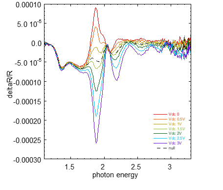
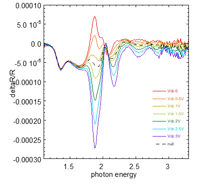
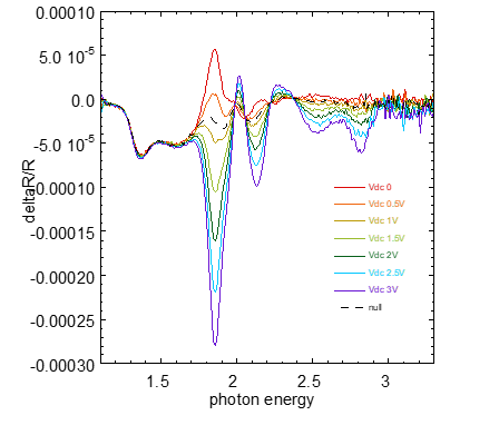
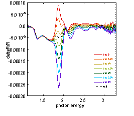
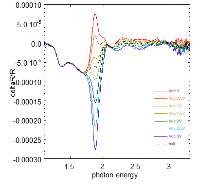
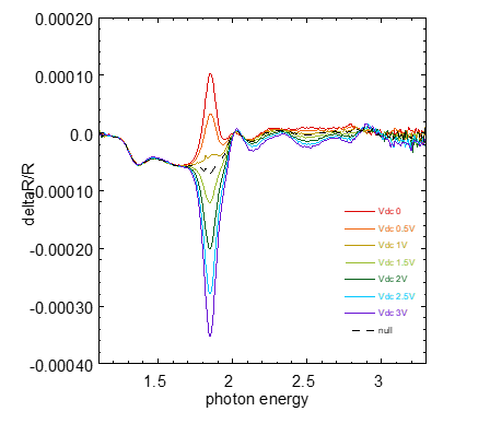
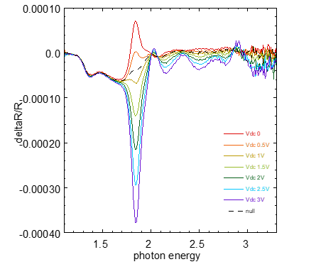
As shown in the figure below, by changing the input value in the data, when the null current curve flips, the voltage value at the flip point is .

By comparing the values of the CB solution system at RT and 60oC, it can be inferred that theVbi at 100oC is close to the theoretical value of 1.2 V. Therefore, EA measurement for the 100oCdevices is not necessary. After obtaining the specific of the device, the carrier mobility can bequantified using the Mott - Gurney law.
Although the Mott-Gurney law can directly provide an equation for carrier mobility, its applicationrequires several ideal conditions, such as a uniform electric field, trap-free transport, and currentdominated by SCLC.
Pasveer demonstrated that in disordered organic semiconductors, the carrier mobility uisdependent on both the local carrier density p and the electric field E. Neglecting these dependencesmay lead to an inaccurate estimation of carrier mobility. Therefore, a modified form of the Mott-Gurney law is required to obtain a more reliable value of carrier mobility. In this study, thederivation was carried out based on Gauss's law and the drift -diffusion equation to better describethe physical processes in the device and obtain more reliable mobility values. The derivationproceeds as follows:
Gauss’s Law: , in 1D: .
MG equation: .
Drift-diffusion equation:
Integrate, we can get
Since we assume the electric field across OSC is constant, we can ignore the term, and:
From Gauss’s Law, we can calculate the carrier density:
The average carrier density is:
In Mott-Gurney regime:
The final result is:
How solvent effect aggregation
For polymer systems, solvents are generally classified as either good solvents or poor solvents. In a good solvent, strong polymer–solvent interactions enable effective solvation of the polymer chains, such that the chains adopt relatively extended conformations and remain well dispersed, with only a weak tendency toward aggregation. By contrast, in a poor solvent, polymer–solvent interactions are comparatively weak, while interchain interactions become more significant. Under these conditions, the polymer chains tend to contract, entangle, and aggregate, and may eventually precipitate from solution.
For conjugated polymers, however, this binary classification is often insufficient to describe their solution behavior in a comprehensive manner. Zhao et al. introduced the concept of a borderline solvent, defined as a solvent with a solvating ability intermediate between that of a good solvent and a poor solvent. In such a medium, the polymer chains are not fully extended and uniformly dispersed, as would be expected in a good solvent. Instead, they are more prone to intermolecular approach and the formation of a certain degree of ordered aggregation, while remaining dispersed in solution without obvious precipitation. Borderline solvents therefore have particular significance in the regulation of aggregation in conjugated polymer systems, and consequently exert an important influence on subsequent film formation, thin-film morphology, and device performance.
As shown in Figure 4, Zhao et al. proposed a mechanism by which a borderline solvent can induce ordered aggregation in conjugated polymers. In a borderline solvent, the polymer chains are more likely to undergo an early transition from coil-like conformations to more extended chain conformations, and subsequently form small, ordered 𝜋-stacking aggregates. These initial aggregates can then further organize and grow into more distinct plate-like stacked structures with a high degree of order and a preferred orientation. During the subsequent spin-coating process, the aggregates continue to spread, develop, and align on the substrate, thereby promoting the formation of an ordered thin film. Zhao et al. suggested that such dilute-solution 𝜋-stacking and the resulting extended-chain aggregates are crucial for achieving pronounced lamellar order in conjugated polymer films.
By contrast, in a good solvent, polymer–solvent interactions are sufficiently strong to maintain the polymer chains in a more fully solvated and dispersed state. Under these conditions, significant 𝜋-stacking tends to occur only at a later stage of film formation. At that point, however, the polymer chains have already become more entangled, and the adjacent 𝜋-stacked aggregates are more likely to interpenetrate and entangle with one another. This suppresses the formation of extended-chain 𝜋-stacks and reduces the degree of structural order in the resulting film. Consequently, films processed from a good solvent typically contain a larger fraction of disordered or amorphous regions.
These observations demonstrate that the solvent plays a decisive role in regulating polymer aggregation behavior. It influences not only the conformation and dispersion state of the polymer chains in solution, but also the onset, extent, and degree of order of aggregation during film formation. Therefore, solvent selection is a key factor in controlling polymer aggregation, and it can subsequently affect thin-film morphology and charge-transport properties.

Result of EA
From the theory of EA, Vbi of different device can be measured. Here is the result of EA:
-
 a
a -
 b
b -
 c
c -
 e
e -
 f
f -
 g
g -
 h
h


Result of carrier mobility
Based on the above equations, the carrier mobility was calculated using the J–V curve data, and the results are shown below.


Conclusion
By cross-comparing the charge carrier mobility of devices fabricated with different film thicknesses, for both PBDB-T and PM6, CB is a more suitable solvent than CF. In the CB system, both polymers show better solubility and stronger aggregation in solution, and the corresponding films show higher carrier mobility. In addition, the CB-based results are consistent under different solution conditions: the behavior observed in the 120 nm films can be viewed as an extension of the 180 nm current–carrier density (CCD) results, while solution heating has only a small effect on mobility. These results suggest that, within the processing range studied here, the charge-transport behavior remains relatively stable, and the film morphology is still in a range that is favorable for carrier transport.
Based on these results, it can be suggested that, within a proper range, stronger aggregation is related to higher carrier mobility. It can be inferred from this that, there seems to be an aggregation window, in which increased aggregation helps improve charge transport. This idea is consistent with the aggregation theory proposed by Zhao et al., which suggests that moderate aggregation can improve molecular packing, strengthen interchain coupling, and form more continuous charge-transport pathways.
A possible explanation is that moderate aggregation provides a certain degree of molecular pre-organization before or during film formation. This pre-organization may help the film form more ordered molecular packing and better-connected transport pathways, which is beneficial for carrier transport. However, this positive effect only exists within an intermediate range. When aggregation is too weak, molecular pre-organization is not enough, so π–π stacking forms too late during film formation, which may lead to chain entanglement, lower order, and poor pathway connectivity. In contrast, when aggregation becomes too strong, the polymer may form overly large domains, fibers, or particles too early, leading to morphology that is less uniform, weaker connection between domains, and more defects or trap effects. As a result, once the aggregation strength goes beyond the proper window, the benefit from better local order may be offset by the loss of film uniformity and long-range transport continuity, and the mobility may decrease.
References
Zhou Mi. Energy Level Alignment in Semiconducting Organic Electronic Devices. A dissertation submitted for the degree of Doctor of Philosophy, Department of Physics National University of Singapore, July 2010.