EA Spectroscopy as a series of sensors: Investigating the Impact of Solvent Type on Mobility in Organic Diodes: Difference between revisions
| Line 11: | Line 11: | ||
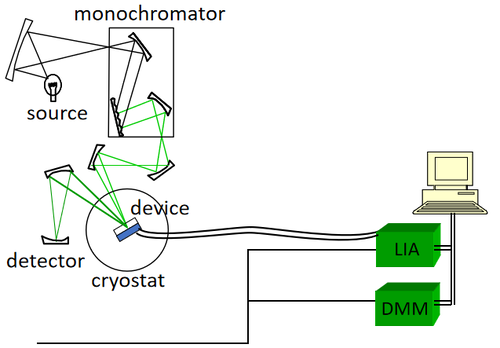
==Schematic diagram== | ==Schematic diagram== | ||
[[File:Optical path diagram.png|500px|thumb|center|Fig1. Optical path diagram]] | |||
==Measurement Process== | ==Measurement Process== | ||
Revision as of 13:04, 28 January 2026
Team members
Li Jinhan A0327554Y
Liu Chenyang A0328377R
Idea
We will use EA spectroscopy, which will include optical sensors, electrical sensors, and lock-in amplifiers, among other components as a highly sensitive, non-destructive optical sensing platform to measure the internal electric field modulation response of organic diodes under operating conditions, and to quantitatively extract carrier mobility based on this measurement. By systematically controlling the thin film preparation temperature and comparing the EA response characteristics of different samples, the project aims to reveal the influence of film preparation temperature on device mobility.
Introduction
The performance of organic semiconductor devices (such as organic diodes) is largely limited by the charge transport processes within the thin film, and carrier mobility is one of the key parameters characterizing charge transport capability. Since organic thin films typically exhibit significant morphological and microstructure sensitivity, the film fabrication temperature affects factors such as molecular packing, crystallinity, phase separation behavior, and trapped state density, thereby altering the internal electric field distribution and charge injection/transport efficiency, ultimately manifesting as differences in mobility and device response. Therefore, establishing a characterization method capable of reliably tracking the "process-structure-transport" relationship is crucial for process optimization and device performance improvement.
Schematic diagram
