LED based avalanched photodetector
Group members:
Cai Shijie
Email:E1184418@u.nus.edu.sg
Nie Huanxin
Email: E1352877@u.nus.edu.sg
Yang Runzhi
Email:E1127408@u.nus.edu.sg
Idea
Our project aims to construct a photo detector to measure some phenomena in optical experiment. We choose Poisson distribution of photons generated by LED as our target phenomena. In the sensor part, we want to detect number of photons, thus we choose reversed LED as the sensor. Using avalanche effect in LED, we could detect relative number of photons with observable quantities.
In the main part, we constructed this LED based avalanched photodetector(APD), explained the working principle and analyzed the result detected by the LED based APD, especially compared the distribution results of photon with theoretical Poisson distribution.
Main
Part 1. Working Principles:
Author: Nie Huanxin
Avalanche Photon detection of Reverse-biased LED
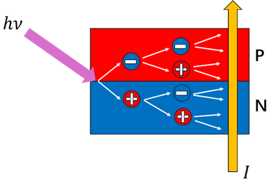
- When a light-emitting diode (LED) light bulb is forward-biased,electrons from the n-region and holes from the p-region migrate toward the depletion zone under the applied electric field. Upon recombination in the active region, energy is released as photons via radiative recombination of charge carriers, converting electrical energy into light—the fundamental principle of LEDs. However, under reverse bias , the LED operates as a photodetector: In the absence of incident photons, the depletion region in LED widens and the built-in electric field is strengthened. Although minority carrier diffusion increases, the absence of photogenerated free carriers results in negligible current (limited only by intrinsic thermal generation). When photons with energy exceeding the bandgap (ℎ𝜈 ≥ 𝐸𝑔) are absorbed, electron-hole pairs (EHPs) will be generated within the depletion zone and separated by strong built-in electric field, then the reverse-biased LED light bulb will operates as a photodetector with distinct voltage-dependent response regimes:
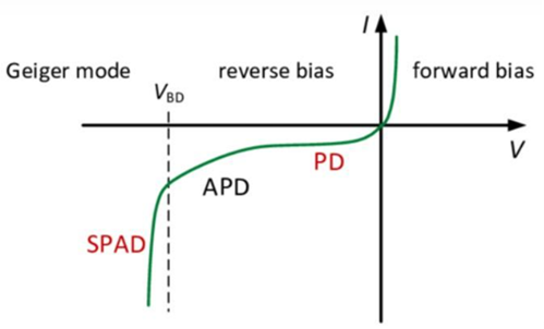
- At small reverse voltages (below the avalanche threshold ), the photocurrent exhibits a near-linear relationship with the applied bias. The observed signal is dominated by leakage current, where photogenerated EHPs are separated by built-in electric field but with negligible current gain. Only primary photocurrent generated from adequate incident photon flux can be detected under this voltage region.
- When approaches the avalanche threshold, the LED turns into Avalanche Photodiode mode, or APD mode. High-energy photogenerated charge carriers in the material gain sufficient kinetic energy to create secondary EHPs via collisions with other carriers, leading to a detectable amplification of the total photocurrent depending on the applied voltage.
- Beyond the breakdown voltage (), the LED operates in Single Photon Avalanche Diode (SPAD) mode, even a single photon can trigger avalanche impact ionization, creating a macroscopic current pulse. SPAD mode have infinitely effective gain, however, the detectable gain is limited by noise, electric loss and quenching.
- In avalanche multiplication regimes, a critical challenge arises when the signal amplification rate exceeds the current decay rate, leading to persistent conduction and preventing subsequent photon detection. Trapped carriers (e.g., at defect sites) during current decay will also trigger false secondary avalanches (afterpulse). To mitigate these effects, quenching is required to reset the diode to its pre-avalanche state. The simplest quenching method employs a series resistor to suppress the avalanche: During an avalanche, the stimulated high current induces a voltage drop across , reducing the bias voltage across the diode below its breakdown threshold (). This terminates the avalanche, allowing the diode to recover. Once the photocurrent ceases, the bias voltage across the diode returns to its original value, ready for the next photondetection. The effectiveness of quenching largely depends on the resistor : If is too small for a sufficient voltage drop, the detection accuracy will be greatly degraded due to the inefficiency of quenching; If is too large, the amplitude as well as time span of signal pulses may be , owning to unqualified signal waves; Only proper can optimize the photodetection efficiency.
- During Experiments, we applied R0=10kΩ empirically for reverse-biased AND 113 LED, to balance quenching efficiency and timing resolution. Also, the LED's reverse-bias range of ∈[25.5V,26.4V] are discovered experimentally, where:
- Below 25.5 V, the field is too weak for detectable gain;
- Above 26.4 V, passive quenching fails to suppress runaway avalanches.
- From the derivations mentioned above, the photodetection mechanism sequence in a reverse-biased LED of APD mode are as follows:
- An incident photon (with energy hν≥Eg) generates an electron-hole pair (EHP) within the depletion region.
- The high electric field accelerates the primary carriers, enabling impact ionization. Secondary EHPs are created through collisions with the lattice, causing an exponential rise in carrier density (n). The resulting current (I) grows exponentially until reaching a peak value ().
- The peak current occurs when the avalanche generation rate balances the recombination rate. At this point, the current is proportional to the carrier density in the photodetector:
Where is temperature-dependent mean free time, and e are the mass and charge of a electron. Under certain temperature T, the is determined by only. - The voltage drop across reduces the bias below , suppressing the avalanche. The diode then behaves as a discharging capacitor, with the current decaying to zero as the system resets to its pre-avalanche state.
Photon detection circuit
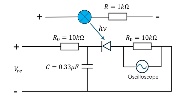
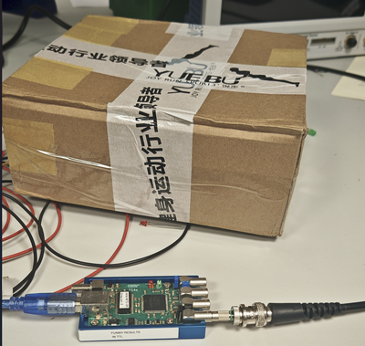
- Theoretically, every reverse-biased LED have a photodetection range near its breakdown voltage . However, only the AND113 red LED exhibits an ideal photodetection voltage range below 30V, making it suitable for experimental applications. And photoelectric conversion efficiency depends on the strength of the LED’s built-in electric field, which is governed by the carrier concentration in the doped semiconductor material. A higher carrier density enhances the internal electric field in depletion zone, thereby improving the separation and collection efficiency of photogenerated electron-hole pairs. To minimize interference from ambient light, measurements were conducted inside a lightproof enclosure (a cardboard box) within a darkroom. Additionally, a series RC low-pass filter was integrated into the photodetection circuit to suppress high-frequency noise arising from residual transient photocurrent signals.
Calculation of quenching equivalent capacitance circuit
- During quenching period, the reverse-biased LED functions as a capacitor:
- So the theoretical relaxation time of such equavalent circuit can be calculated using a second-order RC circuit differential equation:
- where
- However, the width and charge density of depletion zone is determined by the reverse voltage applied on the PN junction, leading to the variation of . Using parallel plate capacitor model, we can derive as a function of . The width of depletion zone W can be expressed as:
- Where ε is the dielectric constant of the material, is the built-in electric field voltage, and is the charge carrier density in P and N zone. Simplifying the formula with approximate carrier density , we can obtain:
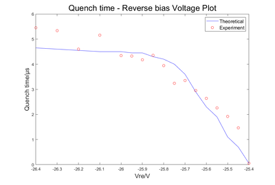
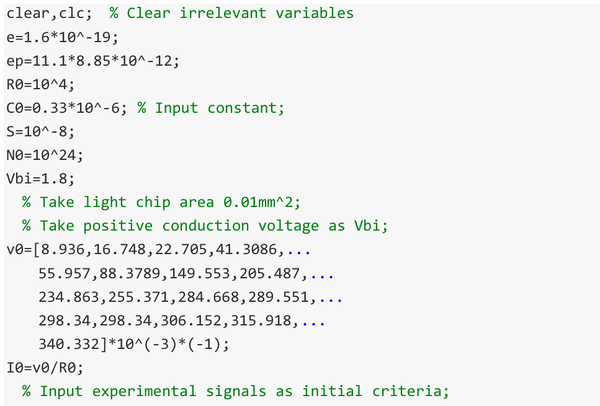
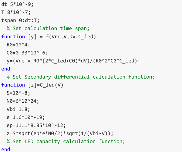
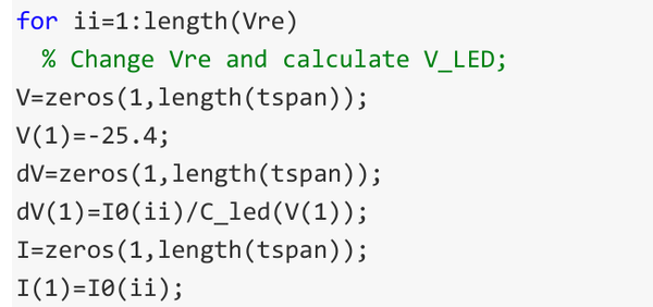
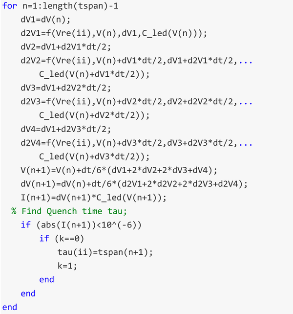
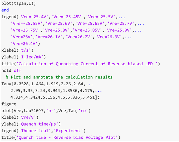
- Since the capacitance is a non-linear function of V_LED, it is extremely difficult to solve the circuit equation directly; instead, translating the equation into numerical calculation programme in MATLAB makes it easier to visualize the theoretical calculation result, which is relatively close to experimental results:
Part 2. Experimental Setup
Author: Yang Runzhi
Equipment and the circuit
Equipment:
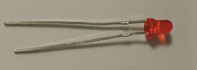
Core: One red LDE , one blue LDE.
KEITHLEY Triple Channel DC Power Supply, ROHDE&SCHWARZ RBT2004 Digital Oscilloscope, Arduino Counter, Multimeter.
Breadboard, resistors, capacitors, wires in all kinds.
We choose a red LED with working wavelength around 650 nm as detector(sensor) and another bule LDE with working wavelength around 450 nm as light source.
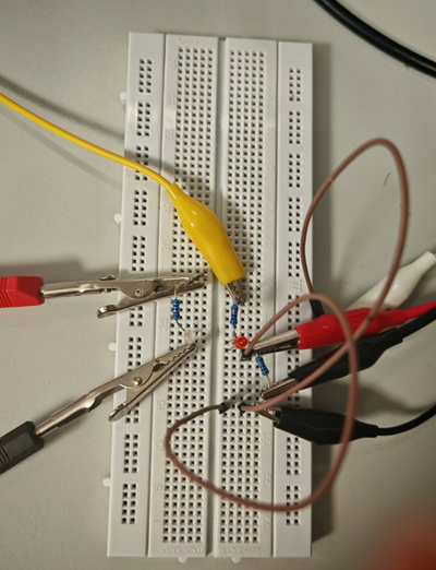
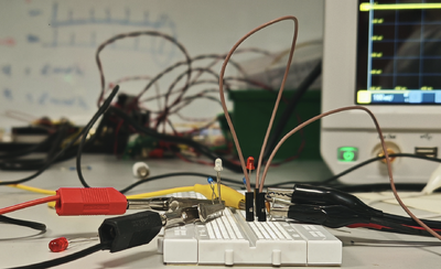
Connect the circuit as the circuit diagram shown in part1.The working voltage and reversed-bias voltage is generated by DC Power Supply. The measure part is connected to either the Oscilloscope or the Counter. The distance between the light source and the detector is 1.3 cm.
The cutoff frequency of a simple RC low-pass filter is given by:
In our case:
Then:
Therefore, the cutoff frequency of the filter is 48.25 Hz. Signals with higher frequency is filtered.
Experiment steps
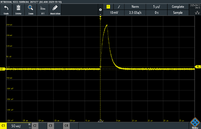
First step is test the working voltage and reversed-bias voltage. Changing the 2 parameter till we can detect excitation in the oscilloscope.
Figure 2.3 is what we got in this step, with working voltage at 5V level and reversed-bias voltage at 25.8V. The figure shows two important parameter which we can detect in the following experiment: height of pulse peaks and decay time after excitations. Also, the number of pulse peaks in a small period is
Then cover the circuit with a box to avoid interference. The effect of this step is that all the photons detector captured are generated by the blue light source.
The main measurement including the following parts:
1.Working voltage sweep: Connect the measure circuit to oscilloscope. Keep the reverse-bias voltage constant at 25.8 V and vary the working voltage from 3 V to 7 V in 0.5 V increments. During each voltage level, use the oscilloscope to measure number of pulses in 1000ms and the height of pulse peaks in 6 times.
2.Reverse-bias voltage sweep: Connect the measure circuit to oscilloscope. Keep the working voltage constant at 5 V and vary the reverse-bias voltage from 25.4 V to 26.5 V in 0.05 V increments. During each voltage level, use the oscilloscope to measure the decay time after excitation.
3.Confirmation the Poisson distribution: Connect the measure circuit to counter. Keep the reverse-bias voltage constant at 25.8 V and the working voltage constant at 5 V. Set the sample time, then sample and compare the sample results with the theoretical Poisson distribution.
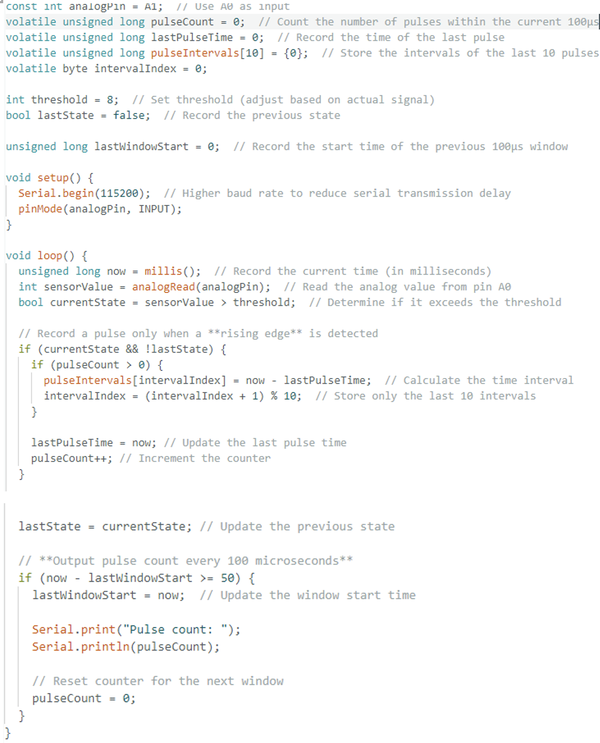
4.Calculate quantum efficiency: Connect the measure circuit to oscilloscope, use the oscilloscope to measure number of pulses in 50ms. Use multimeter to measure the working current and the working voltage of blue LED. Calculate the number of photon generated in 50ms and calculate the quantum efficiency.
Part 3. Results and Analysis
Author: Cai Shijie Date: April 2025
The avalanche effect can be observed with the power of the light source around 13 μW. This indicates that the detector is a sensitive APD capable of detecting low photon number densities.
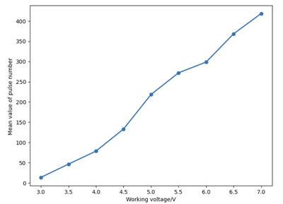
Figure 3.1 measures the average pulse number per 50 ms versus the voltage of the power supply. The linear curve corresponds to the increasing photon number with higher voltage of the light source.
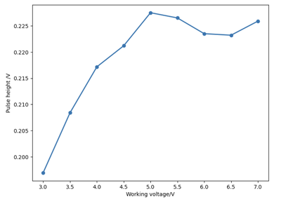
Figure 3.2 shows that the pulse height increases with the voltage of the power supply. For a single-photon avalanche photodiode (SAPD), the curve should be flat, meaning each pulse corresponds to one photon. However, when the power supply voltage is doubled, the pulse height increases significantly, suggesting that each pulse corresponds to several photons.
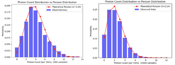
By setting the photocurrent pulse number per 50 ms as one sample, 1000 or 10,000 samples are used for statistical analysis and compared with the theoretical Poisson distribution, resulting in Figure 3.3.
Several methods are used to analyze how closely the data match the theoretical model. The Kullback–Leibler (KL) divergence (result: 0.0061), Jensen–Shannon (JS) divergence (result: 0.0366), and Bhattacharyya distance (result: 0.0014) all qualitatively estimate the similarity between the real data and the theoretical Poisson distribution. All results are close to 0, indicating a high degree of similarity between the two distributions.
The Kolmogorov–Smirnov (KS) test is used to obtain a p-value, which is more sensitive than the previous methods. The p-value indicates the probability of observing the test statistic under the assumption that the data follow a Poisson distribution. The p-value obtained is 0.0264, which is smaller than 0.05, thus rejecting the Poisson distribution in this test.
Furthermore, the quantum efficiency (QE) is estimated by 0.245%. The Python, Arduino code, and QE calculation are attached in the appendix.
In conclusion, the LED-based APD cannot fully verify the Poisson distribution of the LED source, as it is not a true single-photon detector.
Appendix
QE Estimation
Given Parameters
- Blue LED optical power:
- Wavelength of blue light:
- Photon energy:
- Photon emission rate:
- Emission duration:
- Distance between LEDs:
- Red LED pn-junction radius:
- Entrance area of the pn-junction:
- Solid angle covered by receiving junction:
- Fraction of photons geometrically intercepted:
- Shell transmission rate at 450 nm (approximate):
- Number of detected photo-pulses:
Photons Reaching the pn-Junction in 50 ms:
Conclusion: Using a realistic pn-junction area and accounting for geometric and spectral filtering factors, the estimated quantum efficiency of the red LED functioning as a photon detector is approximately 0.245%. This aligns with expectations given that LEDs are not optimized for photodetection, especially under off-band excitation (blue light in a red LED).
Code Listings
