Photodetector with wavelength @ 780nm and 1560nm
Photodetector with wavelength @ 780nm and 1560nm
Team members: Sunke Lan
To design photodetector as power monitor with power within 10mW.
Project Outline
1. Objective
- Design and evaluate photodetectors for 780 nm and 1560 nm applications.
2. Components
- Photodiodes (S5971, G12180-010A)
- BNC and PCB test boards
- Operational amplifier (OP27G) for transimpedance amplification
---
3. 780 nm Photodetector Design
3.1 Circuit and Components Overview
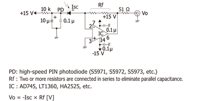
The 780 nm photodetector circuit is based on a standard transimpedance amplifier (TIA) configuration, designed to convert the photocurrent generated by a silicon PIN photodiode (S5971) into a measurable voltage signal.
In this design:
- The photodiode is operated under a reverse bias of 1 V, applied externally to widen the depletion region, reduce junction capacitance, and improve both linearity and response speed. Compared to higher bias voltages (e.g., 15 V), a 1 V bias offers a balance between depletion width and minimized dark current, suitable for steady-state detection at 780 nm.
- The photocurrent generated by incident photons is injected into the inverting input of the OP27G operational amplifier. The amplifier maintains a virtual ground condition at the inverting input, ensuring linear current-to-voltage conversion without significant voltage swing at the photodiode terminal.
- A feedback resistor connects the output to the inverting input, governing the output voltage according to:
where is the photocurrent proportional to the incident optical power.
The OP27G is selected for its excellent low input offset voltage (typically 25 µV), low noise (3 nV/√Hz at 1 kHz), and moderate gain-bandwidth product (8 MHz), making it ideal for precise low-frequency optical measurements.
To ensure stable operation:
- Proper bypass capacitors (0.1 µF ceramic + 10 µF electrolytic) are placed close to the amplifier’s supply pins to suppress high-frequency noise.
- Decoupling capacitors are connected across the photodiode bias supply to stabilize the reverse bias voltage.
 |
 |
This current-to-voltage architecture enables reliable detection of 780 nm light with sufficient sensitivity, stability, and low noise performance for laboratory testing.
3.2 Theory and Circuit Design Concept
The underlying detection principle is the direct conversion of the photogenerated current into a voltage signal using a transimpedance amplifier. By operating the photodiode under reverse bias and maintaining a virtual ground at the amplifier’s inverting input, the circuit ensures linear and efficient current-to-voltage conversion without distorting the photocurrent signal.
The output voltage follows:
where is the photocurrent and is the feedback resistance.
Careful selection of bias conditions, feedback network, and amplifier characteristics optimizes the signal-to-noise ratio and ensures stability within the low-frequency operating range appropriate for 780 nm light detection.
3.3 Feedback Resistor Selection
The feedback resistor determines the transimpedance gain of the photodetector, i.e., the voltage generated per unit photocurrent. A value of was chosen to balance signal amplitude and system stability.
Key considerations include:
- **Signal strength:** Typical photocurrents under 780 nm illumination are in the nanoampere to microampere range. With a 10 kΩ feedback resistor, output voltages reach measurable levels without requiring excessive amplification.
- **Noise performance:** Although increasing amplifies both signal and noise, a 10 kΩ resistor provides a favorable trade-off, maintaining a reasonable signal-to-noise ratio (SNR).
- **Frequency stability:** Larger values, combined with the photodiode’s junction capacitance, can reduce bandwidth and induce phase shifts. A 10 kΩ resistor ensures sufficient stability across the targeted low-frequency range.
Thus, the 10 kΩ feedback resistor enables clean, stable, and easily detectable voltage outputs under typical laboratory conditions.
3.4 Testing and Results
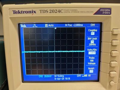
The 780 nm photodetector circuit was tested under indoor lighting conditions to assess its performance. A Tektronix TDS 2024C digital oscilloscope was used to monitor the output under various amplifier supply voltages, capturing the 50 Hz AC mains modulation.
Test results are summarized as follows:
 |
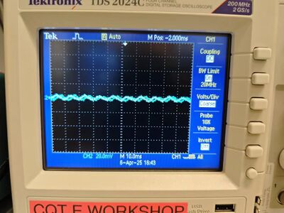
Without amplification, the photodiode output is too weak to be detected by the oscilloscope.
 |
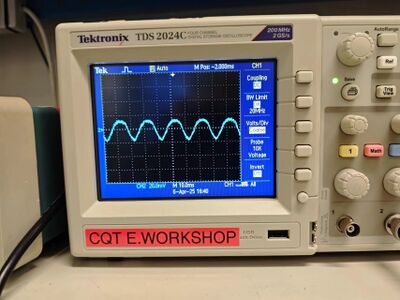
With a ±1 V supply, a small output fluctuation appears, indicating initial amplification.
 |
With a ±3 V supply, a clear quasi-sinusoidal waveform corresponding to 50 Hz ambient lighting is observed, indicating effective amplification.
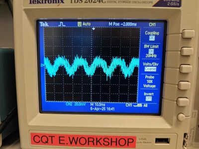 |
At ±5 V, significant distortion and oscillations occur due to instability caused by the combination of weak input signals, high open-loop gain, and parasitic effects from the breadboard assembly.
In summary:
- Without amplification, the photodiode signal remains undetectable.
- A ±3 V supply allows for stable and effective signal amplification.
- Excessive supply voltages (> ±5 V) without proper PCB layout introduce instability.
- The detector demonstrates clear sensitivity to low-frequency ambient light variations.
3.5 Discussion
While the breadboard-based photodetector successfully detects low-frequency optical signals, several limitations exist. Parasitic capacitances and imperfect grounding inherent to the breadboard setup contribute to instability at higher supply voltages. Furthermore, the lack of a fully optimized feedback compensation network restricts bandwidth and dynamic range.
Future improvements include:
- Transitioning to a PCB design to minimize parasitic effects.
- Implementing better shielding against environmental noise.
- Optimizing feedback networks to achieve broader bandwidth and enhanced stability.
These enhancements would enable more precise and higher-speed optical measurements beyond the low-frequency regime demonstrated here.
---
4. G12180 Photodetector Design
4.1 Circuit and Components Overview
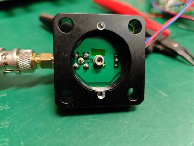
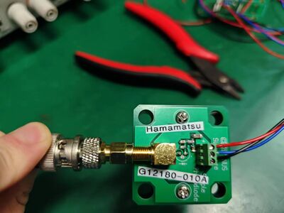
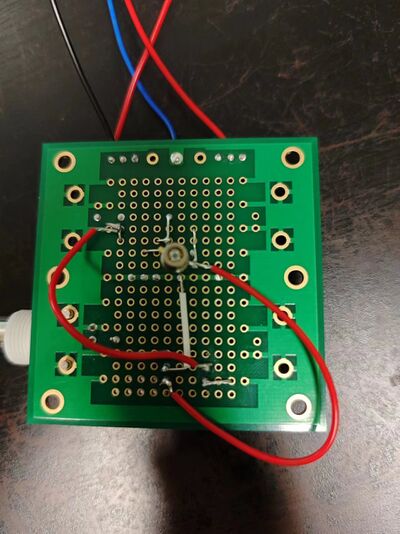
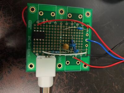
To improve stability and reduce parasitic effects, a dedicated PCB was fabricated for the G12180-010A photodiode. The layout was designed to minimize parasitic capacitance and inductance by shortening trace lengths and optimizing grounding.
The circuit adopts a TIA configuration featuring:
- A 10 kΩ feedback resistor for gain control.
- Bypass capacitors (0.1 µF and 10 µF) near the amplifier supply pins for noise suppression.
- Decoupling capacitors across the photodiode bias supply for voltage stabilization.
The Hamamatsu G12180-010A photodiode is optimized for near-infrared and visible light detection, offering high speed and low noise characteristics.
Mechanical mounting uses a four-screw configuration for optical alignment and stability, with a BNC connector for easy signal extraction.
This setup offers significantly improved stability and sensitivity compared to the breadboard-based design.
4.2 Theory and Circuit Design Concept
The detection principle remains the direct conversion of photocurrent into voltage via a transimpedance amplifier. The PCB design significantly reduces parasitic effects, improves system bandwidth, and enhances immunity to electromagnetic interference (EMI).
The output voltage relation is:
where is the photocurrent and is the feedback resistor.
The PCB-based structure enables cleaner and more accurate optical signal measurements over a broader frequency range.
4.3 Testing and Results
The PCB-based G12180 photodetector was tested under indoor lighting conditions, with output monitored using a Tektronix TDS 2024C oscilloscope.
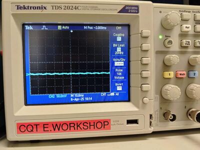 |
As shown, the output signal is highly stable with minimal low-frequency noise. No significant oscillations or distortions were observed, marking a substantial improvement over the breadboard setup.
The enhanced performance is attributed to:
- Reduced parasitic capacitance and inductance.
- Effective bypassing and decoupling.
- Improved grounding and signal integrity through the PCB design.
Overall, the PCB implementation enables clean, low-noise photodetection suitable for both DC and low-frequency optical measurements.