Photodetector with wavelength @ 780nm and 1560nm: Difference between revisions
From PC5271 wiki
Jump to navigationJump to search
| Line 17: | Line 17: | ||
=== 3. Test circuits === | === 3. Test circuits === | ||
==== 3.1.1 Basic current-voltage transferring circuit for S5971 ==== | |||
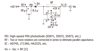
[[File:testcircuit.png|center|thumb|400px|Test Circuit for 780nm Photodetector]] | [[File:testcircuit.png|center|thumb|400px|Test Circuit for 780nm Photodetector]] | ||
Based on the reference circuit, we changed the biase voltage of photodiode to 1V, and used op-amp OP27E to do the current-voltage transferring. | Based on the reference circuit, we changed the biase voltage of photodiode to 1V, and used op-amp OP27E to do the current-voltage transferring. | ||
| Line 25: | Line 25: | ||
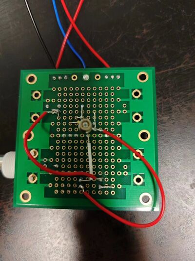
| [[File:front.jpg|400px|thumb|center|the side with basic lump elements]] | | [[File:front.jpg|400px|thumb|center|the side with basic lump elements]] | ||
|} | |} | ||
==== 3.1.2 Theory and Circuit Design Concept ==== | |||
The photodetector circuit in Figure 3-13 is based on the principle of converting the photocurrent generated by the photodiode into a readable voltage signal using a transimpedance amplifier (TIA) configuration. | |||
In this design: | |||
* The photodiode is operated under reverse bias conditions (1 V applied from an external voltage source) to widen the depletion region, reduce junction capacitance, and improve both linearity and response speed. | |||
* The photocurrent generated by incident light is injected into the inverting input of the operational amplifier (OP27G), which maintains a virtual ground at this node. | |||
* A feedback resistor \( R_f = 10\,\mathrm{k}\Omega \) is connected between the output and the inverting input. The output voltage \( V_{\text{out}} \) follows the relation: | |||
<math>V_{\text{out}} = -I_{\text{photo}} \times R_f</math> | |||
* The OP27G is chosen for its low input offset voltage, low noise, and stable operation under moderate gain-bandwidth requirements, making it suitable for low-frequency, steady-state light detection. | |||
* Proper bypass capacitors are added across the amplifier’s power supply terminals to suppress high-frequency noise and prevent self-oscillation. | |||
* Decoupling capacitors are also placed across the bias voltage supply to maintain a stable reverse bias across the photodiode. | |||
This basic current-to-voltage conversion architecture provides a reliable way to monitor light intensities at 780 nm and 1560 nm, ensuring sufficient sensitivity and stability for laboratory testing purposes. | |||
=== 4. Testing and Results === | === 4. Testing and Results === | ||
Revision as of 13:47, 27 April 2025
Photodetector with wavelength @ 780nm and 1560nm
Team members: Sunke Lan
To design photodetector as power monitor with power within 10mW.
Project Outline
1. Objective
- Try to design photodetector for 780nm and 1560nm
2. Components
- Photodiodes (S5917, G12180-010A), BNC test boards, PCB test boards, op-amp (OP27G) (for target 1)
3. Test circuits
3.1.1 Basic current-voltage transferring circuit for S5971

Based on the reference circuit, we changed the biase voltage of photodiode to 1V, and used op-amp OP27E to do the current-voltage transferring.
 |
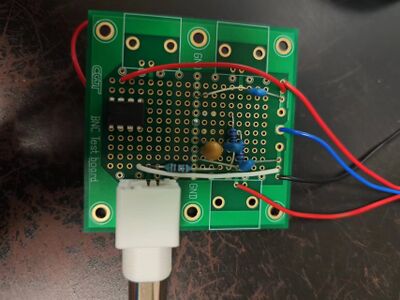
 |
3.1.2 Theory and Circuit Design Concept
The photodetector circuit in Figure 3-13 is based on the principle of converting the photocurrent generated by the photodiode into a readable voltage signal using a transimpedance amplifier (TIA) configuration.
In this design:
- The photodiode is operated under reverse bias conditions (1 V applied from an external voltage source) to widen the depletion region, reduce junction capacitance, and improve both linearity and response speed.
- The photocurrent generated by incident light is injected into the inverting input of the operational amplifier (OP27G), which maintains a virtual ground at this node.
- A feedback resistor \( R_f = 10\,\mathrm{k}\Omega \) is connected between the output and the inverting input. The output voltage \( V_{\text{out}} \) follows the relation:
- The OP27G is chosen for its low input offset voltage, low noise, and stable operation under moderate gain-bandwidth requirements, making it suitable for low-frequency, steady-state light detection.
- Proper bypass capacitors are added across the amplifier’s power supply terminals to suppress high-frequency noise and prevent self-oscillation.
- Decoupling capacitors are also placed across the bias voltage supply to maintain a stable reverse bias across the photodiode.
This basic current-to-voltage conversion architecture provides a reliable way to monitor light intensities at 780 nm and 1560 nm, ensuring sufficient sensitivity and stability for laboratory testing purposes.