Photodetector with wavelength @ 780nm and 1560nm: Difference between revisions
| Line 16: | Line 16: | ||
=== 3. | === 3. 780 nm Photodetector Design === | ||
=== | |||
==== 3.1 Circuit and Components Overview ==== | |||
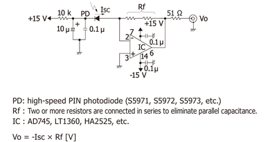
[[File:testcircuit.png|center|thumb|400px|Test Circuit for 780 nm Photodetector]] | |||
The photodetector circuit | The photodetector circuit is based on a standard transimpedance amplifier (TIA) configuration, designed to convert the photocurrent generated by a silicon PIN photodiode (S5971) into a measurable voltage output. | ||
In this design: | In this design: | ||
* The photodiode is operated under reverse bias | * The photodiode is operated under a reverse bias of 1 V, supplied externally, to expand the depletion region, reduce junction capacitance, and enhance linearity and response speed. Compared to higher bias voltages (e.g., 15 V), a 1 V bias provides a trade-off between sufficient depletion width and minimized dark current, which is suitable for steady-state light detection around 780 nm. | ||
* The photocurrent generated by incident | * The photocurrent generated by incident photons is injected into the inverting input of the operational amplifier OP27G. The amplifier maintains a virtual ground condition at the inverting input, ensuring linear current-to-voltage conversion without significant voltage swing at the photodiode terminals. | ||
* A feedback resistor <math>R_f = 10\,\mathrm{k}\Omega</math> is connected between the output and the inverting input. The output voltage | * A feedback resistor <math>R_f = 10\,\mathrm{k}\Omega</math> is connected between the output and the inverting input. The output voltage is governed by: | ||
<math>V_{\text{out}} = -I_{\text{photo}} \times R_f</math> | <math>V_{\text{out}} = -I_{\text{photo}} \times R_f</math> | ||
where \( I_{\text{photo}} \) is the photocurrent proportional to the incident optical power. | |||
* Proper bypass capacitors are | |||
* Decoupling capacitors are | The OP27G was selected for its excellent low input offset voltage (typically 25 µV), low input bias current, and low noise characteristics (3 nV/√Hz at 1 kHz), making it ideal for precise low-frequency optical measurements. Its moderate gain-bandwidth product (8 MHz) provides sufficient speed while maintaining high stability under typical experimental conditions. | ||
To ensure stable operation: | |||
* Proper bypass capacitors (0.1 µF ceramic + 10 µF electrolytic) are placed close to the amplifier’s power supply pins to suppress high-frequency noise and prevent self-oscillation. | |||
* Decoupling capacitors are connected across the 1 V photodiode bias supply to maintain a clean and stable reverse bias, minimizing potential noise coupling. | |||
{| style="width:100%;" | |||
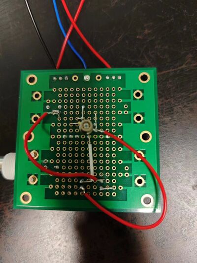
| [[File:back.jpg|400px|thumb|center|Back side with photodiode mounted]] | |||
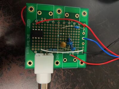
| [[File:front.jpg|400px|thumb|center|Front side with lumped circuit elements]] | |||
|} | |||
This | This current-to-voltage conversion circuit architecture enables reliable detection of light intensities at 780 nm, providing sufficient sensitivity, stability, and low noise performance for laboratory testing and calibration purposes. | ||
=== 4. Testing and Results === | === 4. Testing and Results === | ||
Revision as of 14:00, 27 April 2025
Photodetector with wavelength @ 780nm and 1560nm
Team members: Sunke Lan
To design photodetector as power monitor with power within 10mW.
Project Outline
1. Objective
- Try to design photodetector for 780nm and 1560nm
2. Components
- Photodiodes (S5917, G12180-010A), BNC test boards, PCB test boards, op-amp (OP27G) (for target 1)
3. 780 nm Photodetector Design
3.1 Circuit and Components Overview

The photodetector circuit is based on a standard transimpedance amplifier (TIA) configuration, designed to convert the photocurrent generated by a silicon PIN photodiode (S5971) into a measurable voltage output.
In this design:
- The photodiode is operated under a reverse bias of 1 V, supplied externally, to expand the depletion region, reduce junction capacitance, and enhance linearity and response speed. Compared to higher bias voltages (e.g., 15 V), a 1 V bias provides a trade-off between sufficient depletion width and minimized dark current, which is suitable for steady-state light detection around 780 nm.
- The photocurrent generated by incident photons is injected into the inverting input of the operational amplifier OP27G. The amplifier maintains a virtual ground condition at the inverting input, ensuring linear current-to-voltage conversion without significant voltage swing at the photodiode terminals.
- A feedback resistor is connected between the output and the inverting input. The output voltage is governed by:
where \( I_{\text{photo}} \) is the photocurrent proportional to the incident optical power.
The OP27G was selected for its excellent low input offset voltage (typically 25 µV), low input bias current, and low noise characteristics (3 nV/√Hz at 1 kHz), making it ideal for precise low-frequency optical measurements. Its moderate gain-bandwidth product (8 MHz) provides sufficient speed while maintaining high stability under typical experimental conditions.
To ensure stable operation:
- Proper bypass capacitors (0.1 µF ceramic + 10 µF electrolytic) are placed close to the amplifier’s power supply pins to suppress high-frequency noise and prevent self-oscillation.
- Decoupling capacitors are connected across the 1 V photodiode bias supply to maintain a clean and stable reverse bias, minimizing potential noise coupling.
 |
 |
This current-to-voltage conversion circuit architecture enables reliable detection of light intensities at 780 nm, providing sufficient sensitivity, stability, and low noise performance for laboratory testing and calibration purposes.