Photodetector with wavelength @ 780nm and 1560nm: Difference between revisions
| Line 75: | Line 75: | ||
==== 3.4 Testing and Results ==== | ==== 3.4 Testing and Results ==== | ||
(to be | |||
The photodetector circuit was tested under indoor illumination (standard room lighting driven by AC mains) to evaluate its sensitivity and stability. A Tektronix TDS 2024C digital oscilloscope was used to monitor the output signal under different amplifier supply voltages. The observed signals primarily reflect the 50 Hz modulation from the AC power source. | |||
Test results under different conditions are as follows: | |||
{| style="width:100%;" | |||
| [[File:Test1.jpeg|400px|thumb|center|Output without OP-AMP amplification]] | |||
|} | |||
In the first test, the photodiode was connected directly to the oscilloscope without using the operational amplifier. As shown in the figure, no significant signal was detected. This indicates that the photocurrent generated under normal room lighting is too small (typically in the nanoampere range) to be directly observed by the oscilloscope without amplification. | |||
{| style="width:100%;" | |||
| [[File:Test2.jpeg|400px|thumb|center|Output with OP-AMP supply of ±1 V]] | |||
|} | |||
In the second test, the OP-AMP (OP27G) was powered with a ±1 V supply. A small but noticeable output fluctuation appeared. This result suggests that even with low supply voltage, the amplifier begins to operate and provides a weak but observable amplification of the photocurrent signal. | |||
{| style="width:100%;" | |||
| [[File:Test3.jpeg|400px|thumb|center|Output with OP-AMP supply of ±3 V]] | |||
|} | |||
When the OP-AMP supply voltage was increased to ±3 V, a clear quasi-sinusoidal output waveform emerged. The output signal corresponds to the 50 Hz ambient lighting modulation from the AC mains. This indicates that the photodetector circuit is capable of effectively capturing low-frequency optical signals when properly biased and powered. | |||
{| style="width:100%;" | |||
| [[File:Test4.jpeg|400px|thumb|center|Output with OP-AMP supply of ±5 V]] | |||
|} | |||
At a higher OP-AMP supply voltage of ±5 V, significant output distortion and oscillations were observed. Although the OP27G is designed to operate up to ±15 V, the combination of extremely low input signal (small photocurrent) and high supply voltage led to internal instability, likely due to excessive open-loop gain and insufficient input signal amplitude. Additionally, the use of a solderless breadboard for circuit assembly introduced parasitic capacitances and poor grounding, further exacerbating the instability and promoting self-oscillation at higher supply voltages. | |||
---- | |||
In summary: | |||
* Without OP-AMP amplification, the photodiode signal is too weak to be detected. | |||
* Properly powering the OP-AMP at ±3 V provides clear and stable signal amplification. | |||
* Excessively high supply voltages (beyond ±5 V) without appropriate compensation or PCB layout lead to instability and self-oscillation. | |||
* The photodetector demonstrates good sensitivity to low-frequency ambient light variations when operated under appropriate conditions. | |||
=== 4. Testing and Results === | === 4. Testing and Results === | ||
Revision as of 14:49, 27 April 2025
Photodetector with wavelength @ 780nm and 1560nm
Team members: Sunke Lan
To design photodetector as power monitor with power within 10mW.
Project Outline
1. Objective
- Try to design photodetector for 780nm and 1560nm
2. Components
- Photodiodes (S5917, G12180-010A), BNC test boards, PCB test boards, op-amp (OP27G) (for target 1)
3. 780 nm Photodetector Design
3.1 Circuit and Components Overview
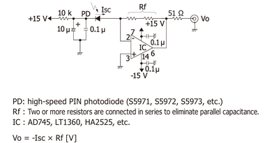
The photodetector circuit is based on a standard transimpedance amplifier (TIA) configuration, designed to convert the photocurrent generated by a silicon PIN photodiode (S5971) into a measurable voltage output.
In this design:
- The photodiode is operated under a reverse bias of 1 V, supplied externally, to expand the depletion region, reduce junction capacitance, and enhance linearity and response speed. Compared to higher bias voltages (e.g., 15 V), a 1 V bias provides a trade-off between sufficient depletion width and minimized dark current, which is suitable for steady-state light detection around 780 nm.
- The photocurrent generated by incident photons is injected into the inverting input of the operational amplifier (OP27G). The amplifier maintains a virtual ground condition at the inverting input, ensuring linear current-to-voltage conversion without significant voltage swing at the photodiode terminals.
- A feedback resistor is connected between the output and the inverting input. The output voltage is governed by:
where is the photocurrent proportional to the incident optical power.
The OP27G was selected for its excellent low input offset voltage (typically 25 µV), low input bias current, and low noise characteristics (3 nV/√Hz at 1 kHz), making it ideal for precise low-frequency optical measurements. Its moderate gain-bandwidth product (8 MHz) provides sufficient speed while maintaining high stability under typical experimental conditions.
To ensure stable operation:
- Proper bypass capacitors (0.1 µF ceramic + 10 µF electrolytic) are placed close to the amplifier’s power supply pins to suppress high-frequency noise and prevent self-oscillation.
- Decoupling capacitors are connected across the 1 V photodiode bias supply to maintain a clean and stable reverse bias, minimizing potential noise coupling.
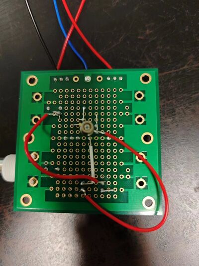 |
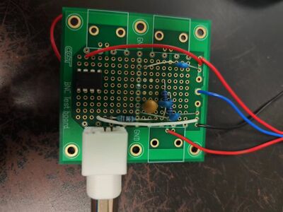 |
This current-to-voltage conversion circuit architecture enables reliable detection of light intensities at 780 nm, providing sufficient sensitivity, stability, and low noise performance for laboratory testing and calibration purposes.
3.2 Theory and Circuit Design Concept
The underlying principle of this photodetector is based on the direct conversion of the photogenerated current into a voltage signal using a transimpedance amplifier structure. By operating the photodiode under reverse bias and maintaining a virtual ground at the amplifier’s inverting input, the circuit ensures linear and efficient current-to-voltage conversion without distorting the photocurrent signal.
The output voltage relationship is given by:
where is the photocurrent proportional to the incident optical power, and is the feedback resistor.
Through careful selection of bias voltage, feedback network, and amplifier characteristics, the circuit optimizes signal-to-noise ratio while maintaining stability across the low-frequency operating range suited for 780 nm light detection.
3.3 Feedback Resistor Selection
The feedback resistor determines the transimpedance gain of the photodetector, i.e., how much voltage is generated per unit of photocurrent. The choice of in this design is a compromise between achieving a sufficient output signal amplitude and maintaining stability against high-frequency oscillations.
Key considerations include:
- **Signal strength:** A typical photocurrent generated under moderate illumination at 780 nm falls in the range of nanoamperes to microamperes. With a 10 kΩ feedback resistor, the corresponding output voltage becomes easily measurable in the millivolt to volt range without requiring excessive amplification stages.
- **Noise performance:** Increasing enhances the signal amplitude but also amplifies thermal (Johnson) noise. A 10 kΩ resistor keeps the noise contribution low while providing an adequate signal-to-noise ratio (SNR) for steady-state measurements.
- **Frequency stability:** Larger values combined with the photodiode’s junction capacitance can reduce the system bandwidth and introduce phase shifts leading to potential oscillations. A 10 kΩ feedback resistor maintains a higher stability margin while covering the low-frequency range of interest in this application.
Overall, a 10 kΩ feedback resistor ensures that the photodetector system delivers clean, stable, and easily detectable voltage outputs under typical laboratory light levels at 780 nm.
3.4 Testing and Results
The photodetector circuit was tested under indoor illumination (standard room lighting driven by AC mains) to evaluate its sensitivity and stability. A Tektronix TDS 2024C digital oscilloscope was used to monitor the output signal under different amplifier supply voltages. The observed signals primarily reflect the 50 Hz modulation from the AC power source.
Test results under different conditions are as follows:
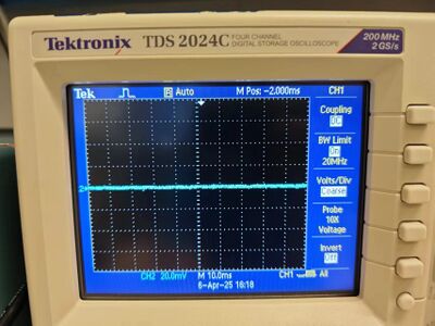 |
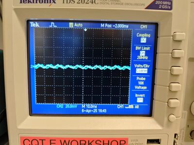
In the first test, the photodiode was connected directly to the oscilloscope without using the operational amplifier. As shown in the figure, no significant signal was detected. This indicates that the photocurrent generated under normal room lighting is too small (typically in the nanoampere range) to be directly observed by the oscilloscope without amplification.
 |
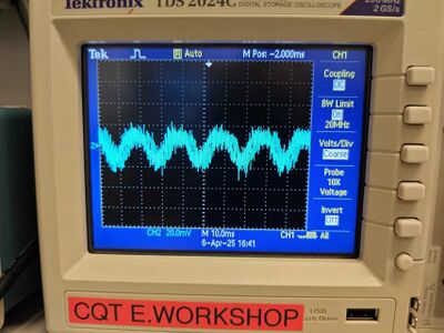
In the second test, the OP-AMP (OP27G) was powered with a ±1 V supply. A small but noticeable output fluctuation appeared. This result suggests that even with low supply voltage, the amplifier begins to operate and provides a weak but observable amplification of the photocurrent signal.
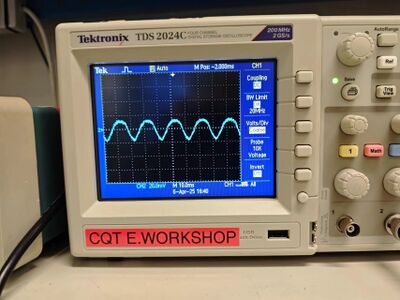 |
When the OP-AMP supply voltage was increased to ±3 V, a clear quasi-sinusoidal output waveform emerged. The output signal corresponds to the 50 Hz ambient lighting modulation from the AC mains. This indicates that the photodetector circuit is capable of effectively capturing low-frequency optical signals when properly biased and powered.
 |
At a higher OP-AMP supply voltage of ±5 V, significant output distortion and oscillations were observed. Although the OP27G is designed to operate up to ±15 V, the combination of extremely low input signal (small photocurrent) and high supply voltage led to internal instability, likely due to excessive open-loop gain and insufficient input signal amplitude. Additionally, the use of a solderless breadboard for circuit assembly introduced parasitic capacitances and poor grounding, further exacerbating the instability and promoting self-oscillation at higher supply voltages.
In summary:
- Without OP-AMP amplification, the photodiode signal is too weak to be detected.
- Properly powering the OP-AMP at ±3 V provides clear and stable signal amplification.
- Excessively high supply voltages (beyond ±5 V) without appropriate compensation or PCB layout lead to instability and self-oscillation.
- The photodetector demonstrates good sensitivity to low-frequency ambient light variations when operated under appropriate conditions.